/ Daily News…
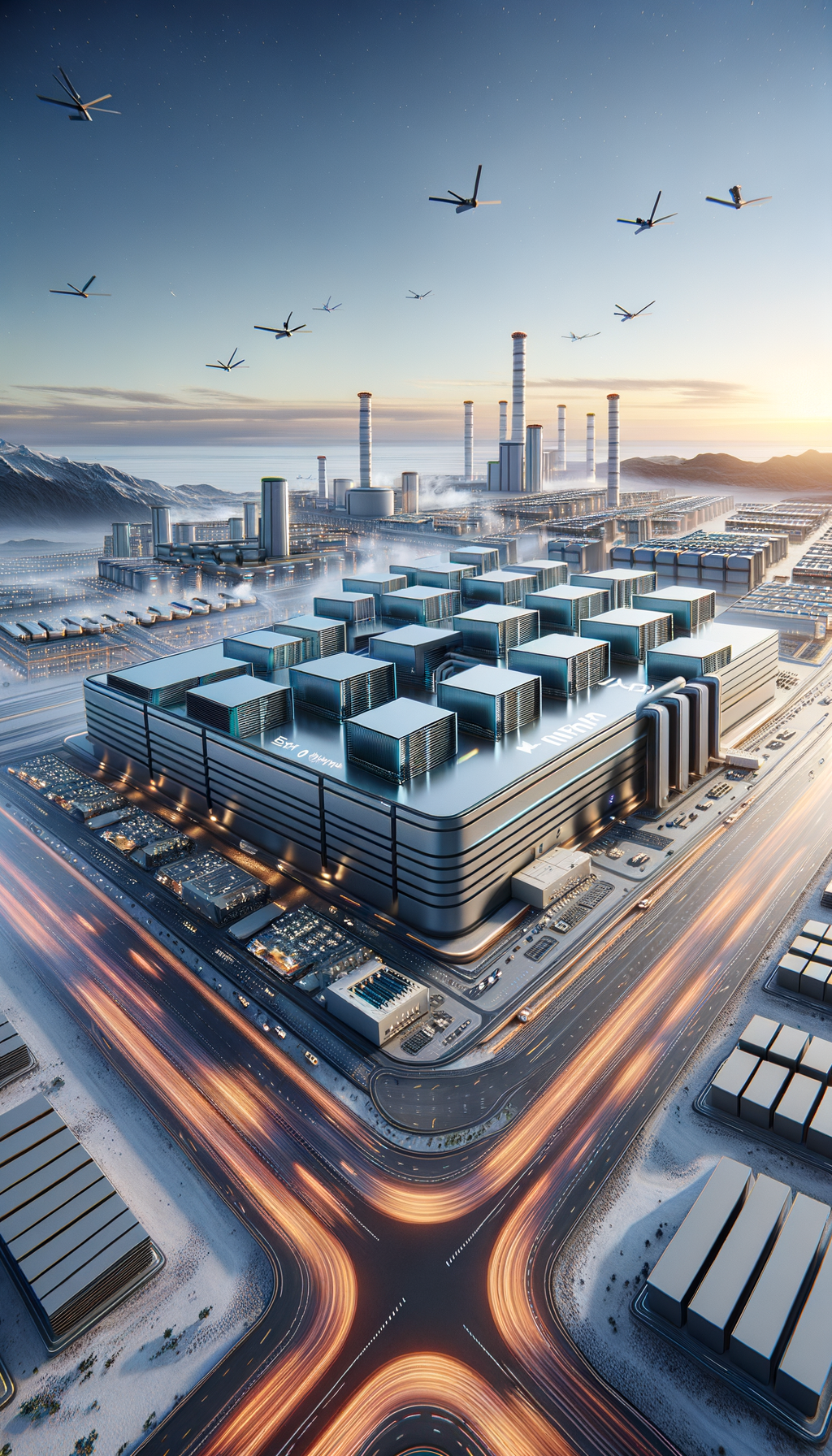
In response to overwhelming demand for high-bandwidth memory (HBM) in AI applications, SK Hynix announced the construction of a $13 billion packaging and testing facility in South Korea. This is part of the company’s effort to meet surging growth in the AI sector. The facility, named P&T7, will be located at the Cheongju Technopolis Industrial Park, with construction starting in April and completion expected by the end of 2027. As HBM becomes crucial in datacenter GPUs and AI accelerators, demand is predicted to grow 33% annually from 2025 to 2030. HBM stacks layers of DRAM to enhance capacity and performance, but its intricate production process makes it costly, with any defects leading to significant financial impacts. This rise in demand has led to climbing memory prices, affecting both consumer and business sectors, while benefiting memory manufacturers like Samsung, Micron, and SK Hynix with increased profits. Despite the facility’s potential to alleviate high demand issues, the benefits for consumer market pricing remain uncertain, with the focus largely on supporting major clients like AMD and Nvidia.
SK Hynix’s New $13B Facility to Boost AI-Driven Memory Production